products


XDB103-9 Series Pressure Sensor Module
Features
1. Error: 1% from 0 ~ 8 5℃
2. Full temperature range ( -40 ~ 125 ℃), error: 2%
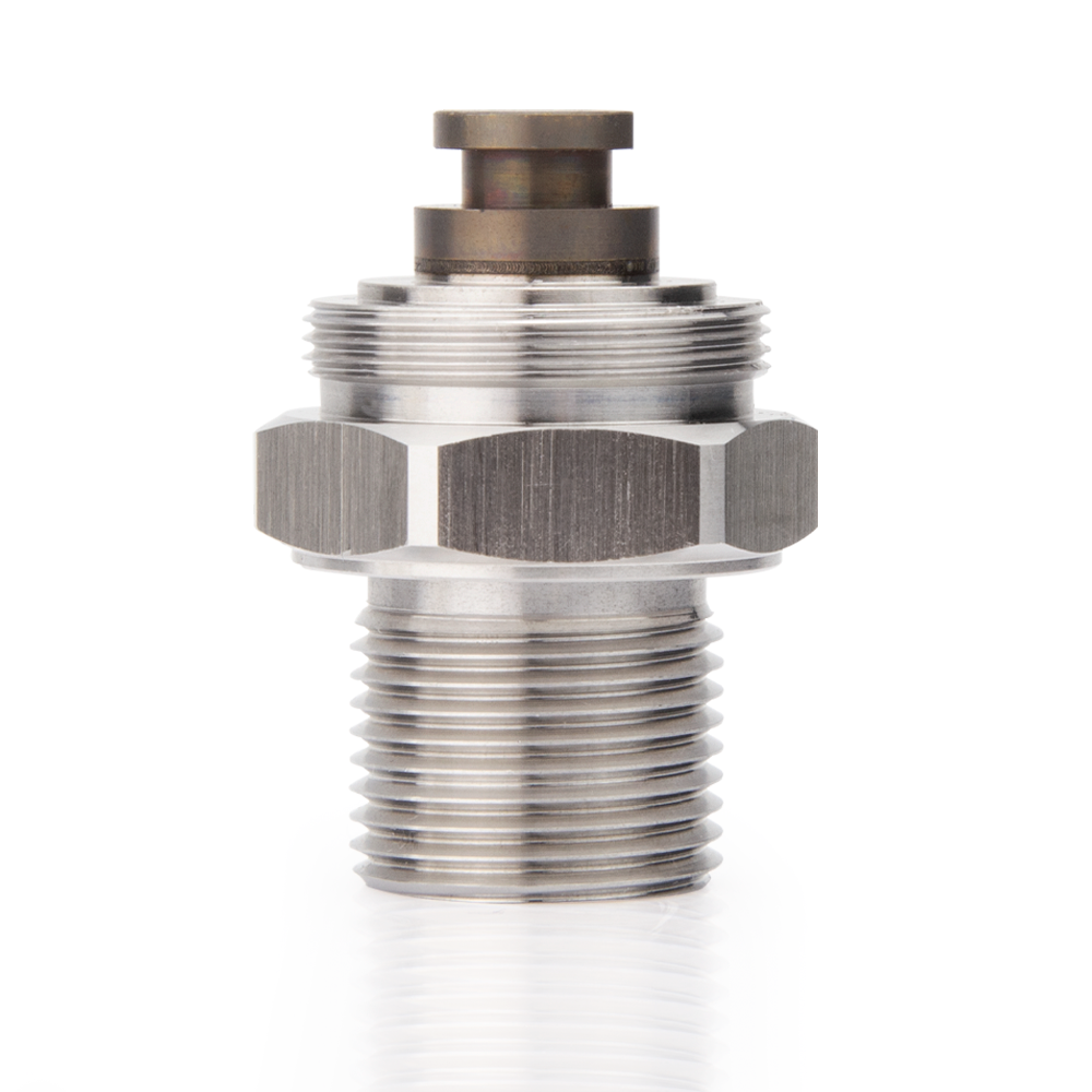
3. Dimensions compatible with typical ceramic piezoresistive sensors
4. Overload pressure: 200% FS, burst pressure: 300%FS
5. Working mode: Gauge pressure
6. Output mode: voltage output and current output
7. Long-term stress drift: <0.5%
Typical applications
1. Commercial vehicle air pressure sensor
2. Oil Pressure Sensor
3. Water pump pressure sensor
4. Air compressor pressure sensor
5. Air conditioning pressure sensor
6. Other pressure sensors in automotive and industrial control fields
Working characteristics

1. Within this operating voltage range, the module's output maintains a proportional and linear relationship.
2. Minimum Pressure Offset: Refers to the module's output voltage at the lowest pressure point within the pressure range.
3. Full-Scale Output: Denotes the module's output voltage at the highest pressure point within the pressure range.
4. Full-Scale Span: Defined as the algebraic difference between the output values at the maximum and minimum pressure points within the pressure range.
5. Accuracy encompasses various factors, including linearity error, temperature hysteresis error, pressure hysteresis error, full-scale temperature error, zero temperature error, and other related errors.
6. Response Time: Indicates the time it takes for the output to transition from 10% to 90% of its theoretical value. Offset Stability: This represents the module's output offset after undergoing 1000 hours of pulse pressure and temperature cycling.
Limit parameters

1. Going beyond the specified maximum ratings can lead to performance deterioration or device damage.
2. The maximum input and output currents are determined by the impedance between the output and both ground and the power supply in the actual circuit.
Electromagnetic compatibility EMC
The product complies with the following EMC testing criteria:
1) Transient pulse interference in power lines
Base norm: ISO7637-2: “Part 2: Electrical transient conduction along supply lines only
| Puls No | Voltage | Function Class |
| 3a | -150V | A |
| 3b | +150V | A |
2) Transient anti-interference of signal lines
Base norm: ISO7637-3: “Part 3: Electrical transient transmission by capacitive and inductive coupling via lines other than Supply lines
Test modes: CCC mode : a = -150V, b = +150V
ICC mode:± 5V
DCC mode:± 23V
Function Class: Class A
3) Radiated immunity RF immunity-AL SE
Base norm: ISO11452-2:2004 "Road vehicles — Component test methods for electrical disturbances from narrowband radiated electromagnetic energy — Part 2: Absorber-lined shielded enclosure ”
Test modes: Low-Frequency Horn Antenna: 400~1000MHz
High gain antenna: 1000~2000 MHz
Test level: 100V/m
Function Class: Class A
4) High current injection RF immunity-BCI ( CBCI )
Base norm: ISO11452-4:2005 “Road vehicles — Component test methods for electrical disturbances from narrowband radiated electromagnetic energy—Part 4:Bulk current injection ( BCI )
Frequency range: 1~400 MHz
Injection probe positions: 150mm, 450mm, 750mm
Test level: 100mA
Function Class: Class A
Transfer function and output characteristic diagrams
1 ) Transfer Function
VOUT = Vs × ( 0.00066667 × PIN +0.1 ) ± ( pressure error × temperature error factor × 0.00066667 × Vs) where Vs is the module supply voltage value, unit Volts.
The PIN is the inlet pressure value, the unit is KPa.
2 ) Input and output characteristics diagram ( VS =5 Vdc , T =0 to 85 ℃)

3 ) temperature error factor

Note: The temperature error factor is linear between -40~0 ℃ and 85~125 ℃.
4) Pressure error limit

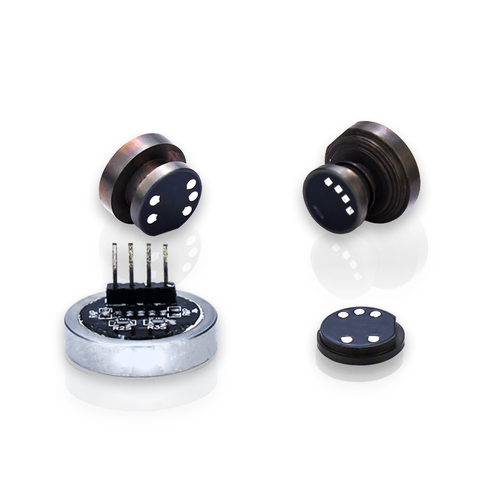
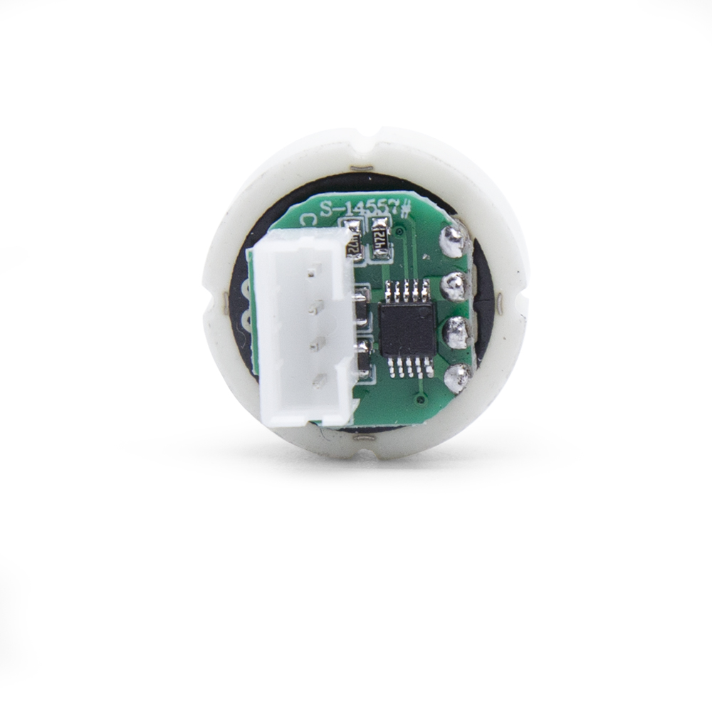
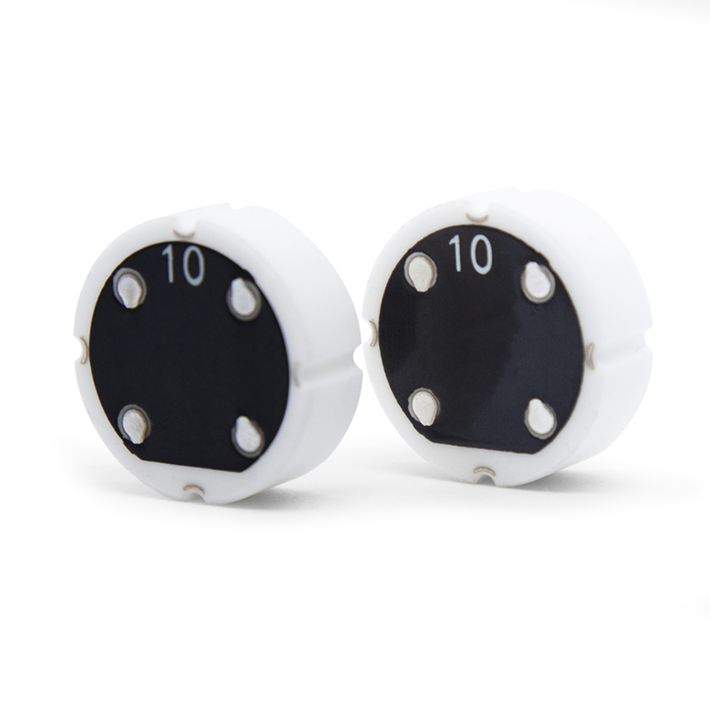
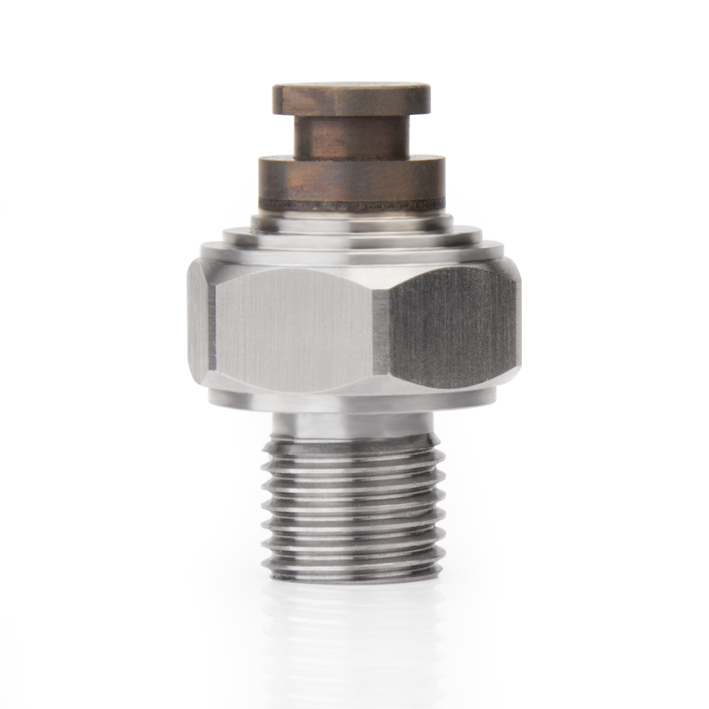
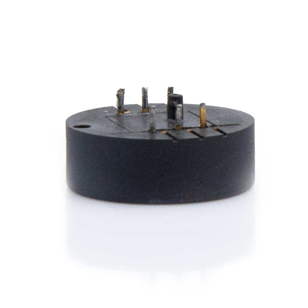
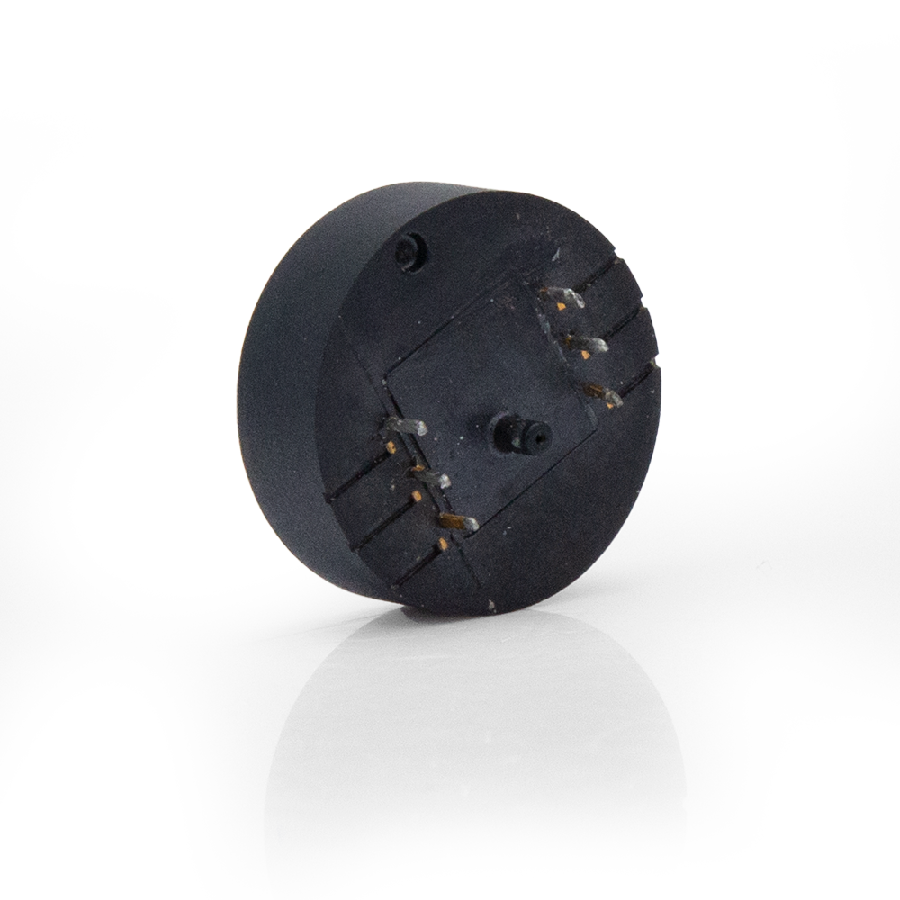
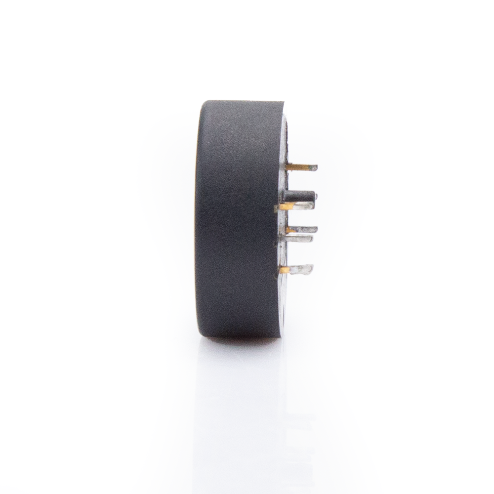
Module dimensions and pin descriptions
1 ) Pressure sensor surface

2) Precautions for Chip Usage:
Due to the unique CMOS manufacturing process and sensor packaging employed in the conditioning circuitry of the chip, it's vital to prevent potential damage from static electricity during your product's assembly. Keep the following considerations in mind:
A) Establish an anti-static safety environment, complete with anti-static workbenches, table mats, floor mats, and operator wristbands.
B) Ensure the grounding of tools and equipment; consider using an anti-static soldering iron for manual soldering.
C) Use anti-static transfer boxes (note that standard plastic and metal containers lack anti-static properties).
D) Due to the sensor chip's packaging characteristics, avoid employing ultrasonic welding processes in your product's manufacturing.
E) Exercise caution during processing to avoid obstructing the chip's air inlets.